SPINNER adapters offer outstanding electrical and mechanical properties
Adapters are used to connect transmission lines with different interface sizes (so-called inter-type or between-lines adapter) or within one size but different interface genders (so-called within-type or in-line adapter).
SPINNER high frequency adapters are optimized for quality and performance and are designed for the lowest possible reflection factors. The outstanding electrical and mechanical properties, the simple installation and the high reliability make SPINNER high-frequency adapters one of the most efficient and cost-effective transition connectors on the market. Precision adaptors with RF quality grade 0 are available upon request.
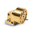
The SPINNER PCB launch connector R 900 (WR 10) 75-110 GHz is characterized by its excellent low IM values and its longevity for test and measurement laboratories. A SPINNER precision adapter increases the lifetime of the connector of the analyzer considerably and thus saves money in the long term.
Outstanding RF characteristics, best possible passive intermodulation and VSWR
A PCB launch connector R 900 (WR 10) 75-110 GHz enables you to reliably transmit radio-frequency signals in the frequency range from 75 to 110 GHz.
The adaptor offers a transition from interface R 900 to interface R 900. The right-angle connector enables installation in confined spaces or special cable inlets.
For interconnection of ordinary waveguides there exists a plurality of waveguide flanges. They are defined in detail by the standards IEC 60154-2, EIA RS-166, EIA RS-271, MIL-DTL-3922, MOD UK DEF-5352and others. These standards also specify the designations for the constructive flange design. The designation lists the type, e.g. flat flange without sealing groove, flat flange with sealing groove or choke flange with sealing groove. Furthermore, the types, i.e. the specific flange geometry (as in EIA and IEC standards) or the part number of a specific flange made of a specific material (as in MIL and DEF standards) are indicated. Finally, the designation of the waveguide is given.
For the specific details, please refer to the SPINNER technical document TD-00077. In addition to these standardized flange designs, there are other specific designs such as LIL (CERN), DESY or Merdinian. The compatibility is indicated in the data sheets.
MIL-Spec flanges have designations of the form UG-xxxx/U where the x's represent a variable-length catalogue number, not in itself containing any information about the flange.